Introduction
This project describes the design, construction, and testing of a 2m foxhunt transmitter for amateur radio. For some background, I recently joined the amateur radio club at UIUC, W9YH. One thing the club doesn’t have currently is a foxhunt transmitter, so I figured it would be a fun project to try and build my own FM transmitter for foxhunting. Foxhunting for the uninformed is where you hide a small radio transmitter somewhere, then use directional antennas to try and find the location of the transmitter. It’s lots of fun and a great learning experience for new hams!
Inspiration
In the past when I was a member at the K5LSU amateur radio club we used the Byonics MicroFox 15. It’s a great transmitter with the following features:
- Operates on any frequency on the 2m band (146-148 MHz)
- Transmits up to 15 mW power
- Uses a 9V battery for power
- Operates for ~20 hours at 50% duty cycle
- Tranmits tone and morse code ID fully configurable with USB cable and Windows software
I really like this transmitter, and want to model this project after it. A key improvement I’d like to make is to increase output power to 50 mW, and also allow the power to be adjustable.
Intro to MAX2606
The MAX2606 is an integrated circuit which implements a voltage controlled oscillator (VCO) which can oscillate from 70-150 MHz, covering the 2m band perfectly. It’s a great IC as it integrates most of the components on the chip. All that’s needed to set the oscillation frequency is an external inductor which sets the nominal oscillation frequency, and an external tuning voltage to trim the frequency output (hence why it’s called a VCO!).
For foxhunting we use handheld radios which receive frequency modulated (FM) signals. To frequency modulate a signal, e.g. one’s voice signal generated by a microphone, we just have to convert the varying voltage of the voice signal to a varying frequency. And since the MAX2606 is a voltage controlled oscillator, it does exactly that! We can then take this FM signal and amplify it using transistors to get our desired 50 mW output power.
Block Diagram Overview
Below is a diagram showing my idea on how to implement this.
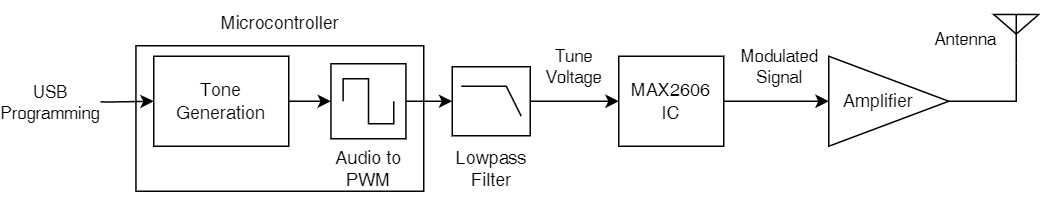
Let’s look at the theory of operation of each section.
Microcontroller
The microcontroller’s purpose is to accept USB programming from a computer, and output pulse width modulated audio. The USB programming could be done by using an Arduino with a USB serial interface. A simple program could be written to write commands to the serial port to program the device, but EEPROM will be needed on the microcontroller to store the settings on power down.
To generate the audio that drives the FM modulator, we first need to generate the audio samples inside of the microcontroller based on the programmed tone and morse code ID desired. Then, the samples can be played using pulse width modulation. Essentially, the amplitude of each sample will determine the width of the pulse, also called the duty cycle (see this Sparkfun article for more info). This is a simple way to output audio digitally with a microcontroller without needing to use a digital-to-analog converter (DAC).
Lowpass Filter
The low pass filter will be used to demodulate the PWM audio generated by the microcontroller. The PWM signal has a fixed frequency, which needs to be sufficiently higher than the audio frequency. However, the duty cycle is not fixed, and varies according to the amplitude of the original audio. Since the duty cycle (time the PWM signal is switched on during one period) is proportional to the amplitude of the audio, then taking the average voltage of each period of the PWM cycle will give the amplitude of the original audio (normalized to the supply voltage). The low pass filter does this by removing the high frequency PWM switching frequency and leaving the average of the duty cycle, thus leaving us with the desired audio. This is the same mechanism Class D amplifiers use, if you’re interested in reading more about this.
MAX2606 IC
The MAX2606 IC, as discussed, will be used as the FM modulator in this project. Below is the pinout of this IC:
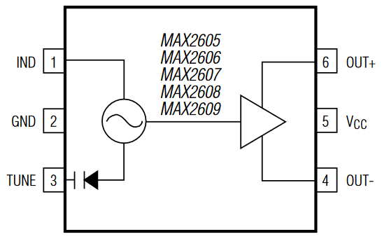
The supply voltage is applied to the VCC pin, which can be up to 5.5 V and as low as 2.7 V. If using a 9 V battery, we can simply use a linear regulator to step this down to 5 V, which will also be convienient for powering the microcontroller. Next, the oscillator output is a differential output from OUT+ to OUT-, but can also be taken single ended from just OUT+ if desired. Since we are amplifying the signal after modulation, we don’t really care about the extra gain and added circuit complexity inherent with a differential output. Thus we will take the output single ended.
For actually setting the oscillation frequency, the IND and TUNE pins are used. To set the fixed oscillation frequency at the mid point of the TUNE voltage, all that is needed is an inductor from IND to GND. Then this fixed frequency can be adjusted by applying a voltage to the TUNE pin.
Regarding the TUNE pin there are two levels of control the audio signal needs to provide to the TUNE pin in order to output the audio on a specific frequency: amplitude and DC offset. The amplitude of the audio will determine the frequency deviation of the FM signal, which is how much the frequency of the FM signal deviates from the carrier in FM. For amateur radio, this is typically +/- 5 kHz. Next, the DC offset will set the carrier frequency of the FM signal, which is the frequency we are transmitting on. So the real questions that need to be answered are:
- How does audio signal amplitude correspond to FM signal deviation?
- How DC offset of the audio signal correspond to the carrier frequency?
Well… We have a partial answer. The datasheet provides us with this graph showing the correlation between the TUNE voltage and the output frequency, but only for a specfic evaluation kit with VCC = 2.75 V and the TUNE voltage adjusted from 0 to 2.75 V!
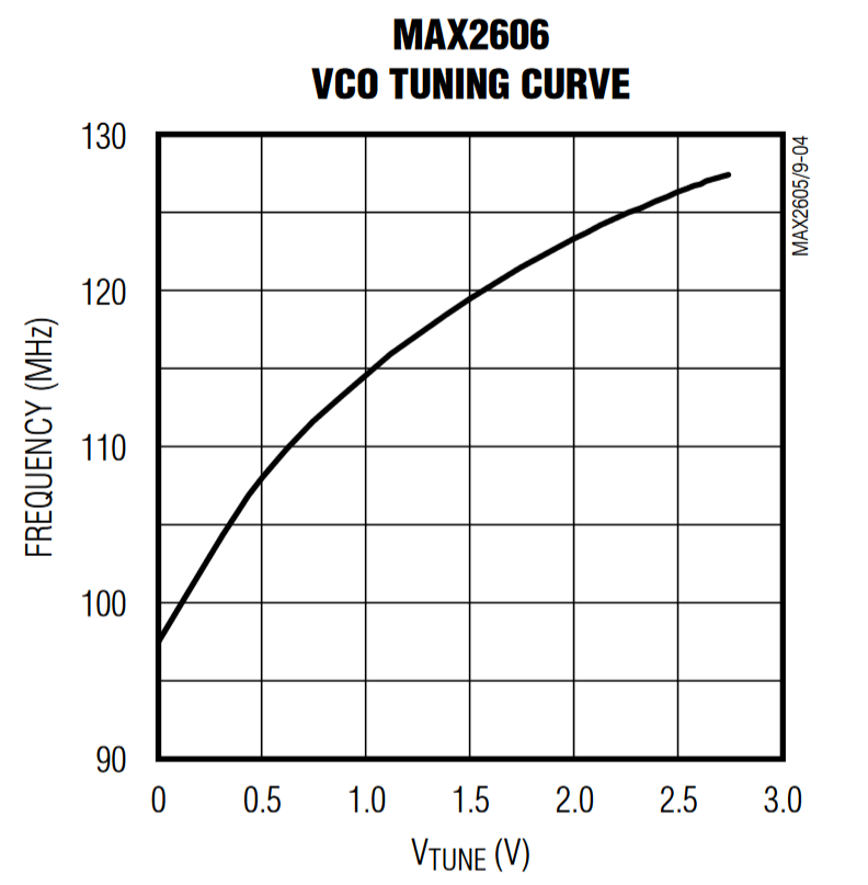
So, we will need to build a test circuit using our VCC of 5 V and an appropriately selected inductor and gather some empirical data to find the tuning curve for our application. We see the graph above is especially not useful to us as the evaluation kit can’t even tune to the desired frequency we want (146-148 MHz).
Amplifier/Antenna
The amplifier’s job is to take the VCO output from the MAX2606, amplify it so that the output power is 50 mW, and feed that to the antenna so it can be transmitted. For the amplifier, I’d like to try and design a BJT amplifier. The amount of gain and stages the amplifier uses will depend on the output voltage from the MAX2606, which will be determined later. I want to keep the output amplifier as simple as possible, so if one amplifier stage gets the job done then I will only use one stage. But this part will be a big learning experience for me since I’ve never designed amplifiers for this frequency. Hopefully simple BJTs like 2N2222 or 2N3904 can be used to keep things simple.
As for the antenna, the output of the amplifier will be connected to an SMA connector which will allow any commercially available amateur radio antenna for the 2m band to be connected. Since most antennas have a 50 Ohm impedance at their operating frequency, the amplifier’s output impedance should be matched to this.
And voila! That’s the theory of operation of the transmitter. Let’s get into the design.
MAX2606 Test Circuit
First, we need to design a test circuit to characterize the MAX2606 using the specifics of our circuit. The requirements are to generate a 146 MHz fixed frequency at VCC = 5 V. Let’s design the circuit using the datasheet.
Inductor Selection
First, we need to select an inductor that gives us a center freqquency of the middle of the 2m band. Since the band spans from 144-148 MHz, 146 MHz will be the center of the band. The datasheet gives the following curve of oscillation frequency vs inductance:
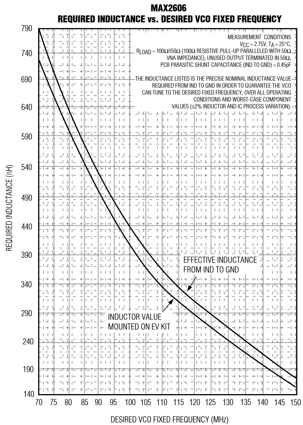
Note that two curves are provided. One for the inductor value mounted on the specific evaluation kit they used to characterize the device, and one for the effective inductance from IND to GND. We should use the effective inductance curve since we are not using the evaluation kit. The effective inductance curve shows what the fixed VCO frequency will be according to the total inductance seen at the IND pin, which is the sum of the inductor we select and any parasitic inductance. Then 146 MHz corresponds to an effective inductance of slightly less than 190 nH.
If we assume there is approximately 10 nH of parasitic inductance, then we should choose 180 nH as the inductor value, which coincidentally is a standard value. If we have more parasitic inductance, we need a lower inductance. To account for this in our test circuit we can select the next inductance down (150 nH) then place lower value inductances in series with the 150 nH to test which gives a 146 MHz oscillation frequency. This is actually the method the datasheet describes in the case that the required inductance is a non standard value. We should also note that the Q of the inductor selected must be >35 for the MAX2606.
TUNE Pin Bypass Capacitor
According to the datasheet, a bypass capacitor must be placed from TUNE to GND. This bypass capacitor provides essentially a short to ground for AC signals at the cathode of the varactor which is at the TUNE pin. The datasheet provides that this must be at least 680 pF and must have a low loss dielectric like NP0. since the datasheet says it is appropriate to select the next standard value up, we will use 1 nF since that is very available and cheap using NP0 dielectric. This capacitance is low enough that it will present a sufficiently high impedance to the audio signal and not draw too much current from the filter and microcontroller.
Output Circuit
Since the MAX2606 uses a differential output, some additional care must be taken in handling the output. Another important aspect is that the output pins are open collector, and thus need pull up resistors to VCC to allow a voltage to be generated at the output pins due to the current drawn by the collectors of the output transistors. The datasheet states that 1 kOhm resistors are the maximum value that can be used to keep the output voltage swing within compliance of the max allowed voltage on the output pins. Thus we will simply use 1 kOhm pullup resistors on both OUT+ and OUT- to VCC.
Rather than take the output differentially, which would require a differential amplifier to be designed for interfacing with the amplifier stage, we can just take the output voltage from OUT+ to GND. This essentially completes the bare minimum design of the basic test circuit.
Other Considerations
Other considerations to take note of is that like with any integrated circuit, we should provide a decoupling capacitor very close to the IC between VCC and GND to allow the IC to source adequate current during high frequency transients. The standard value is 100 nF which will be used here.
In addition, we need a very stable supply voltage as variations in the supply will cause output frequency to shift. Refer to the “supply pushing” characteristic in the datasheet for more info on this. Since we are using a 9 V battery, this gives us good stability already. To make a 5 V supply from the battery, a linear regulator will be used to step this down to 5 V without generating extra noise. In this case the LM78L05 regulator will be used.
Final Test Circuit Design
To be posted in the next update. Stay tuned!